- 您现在的位置:买卖IC网 > Sheet目录316 > BU9883FV-WE2 (Rohm Semiconductor)IC EEPROM 6KBIT 400KHZ SSOP16
�� �
�
�BU9883FV-W�
�Datasheet�
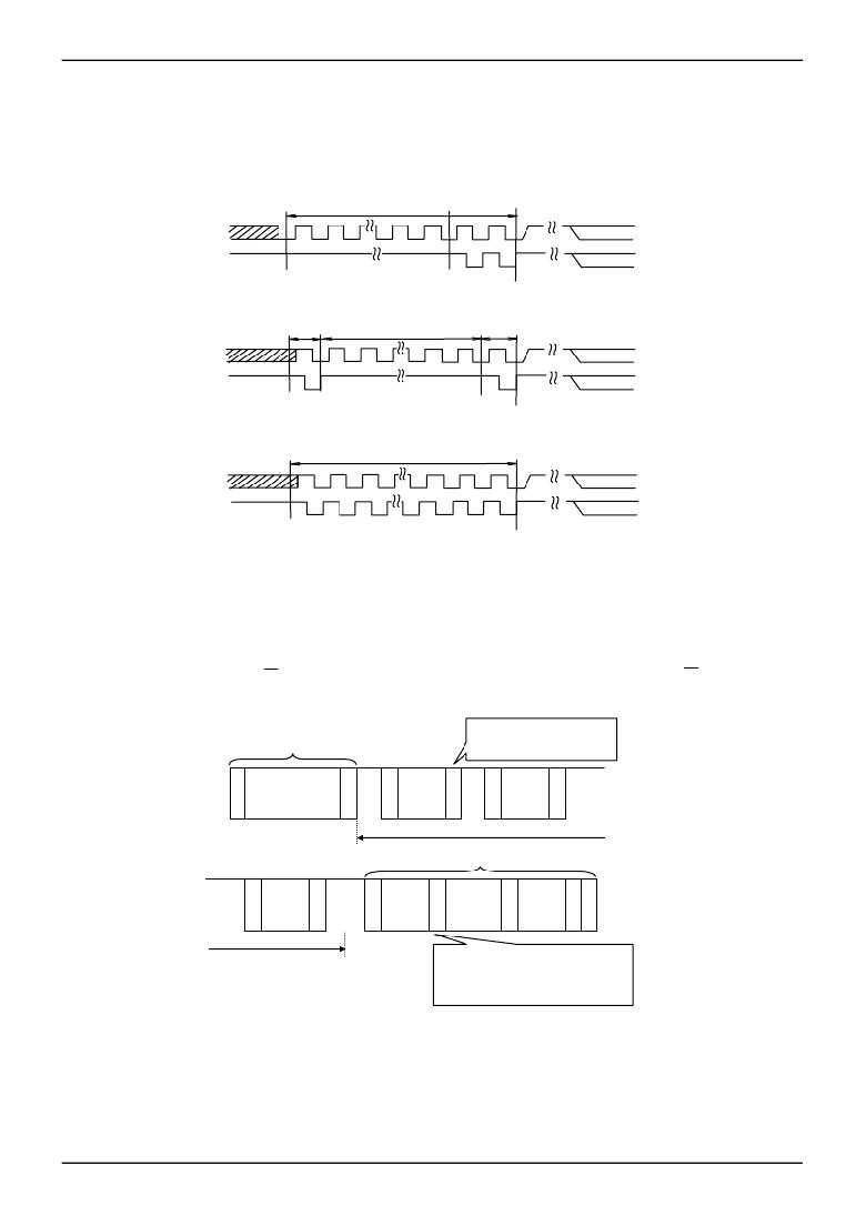
�●� Software� reset�
�Software� reset� is� executed� when� to� avoid� malfunction� after� power� on,� and� to� reset� during� command� input.� Software� reset�
�has� several� kinds,� and� 3� kinds� of� them� are� shown� in� the� figure� below.� (Refer� to� Figure� 47-(a),� Figure� 47-(b),� and� Figure� 47-�
�(c).)� In� dummy� clock� input� area,� release� the� SDA0� to� 3� buses� ('H'� by� pull� up).� In� dummy� clock� area,� ACK� output� and� read�
�data� '0'� (both� 'L'� level)� may� be� output� from� EEPROM,� therefore,� if� 'H'� is� input� forcibly,� output� may� conflict� and� over� current�
�may� flow,� leading� to� instantaneous� power� failure� of� system� power� source� or� influence� upon� devices.�
�Dummy� clock×14�
�Start×2�
�SCL0� to� 3�
�1�
�2�
�13�
�14�
�Normal� command�
�SDA0� to� 3�
�Normal� command�
�Figure� 47-(a)� The� case� of� dummy� clock� +START+START+� command� input�
�Start�
�Dummy� clock×9�
�Start�
�SCL0� to� 3�
�1�
�2�
�8�
�9�
�Normal� command�
�SDA0� to� 3�
�Normal� command�
�Figure� 47-(b)� The� case� of� START� +9� dummy� clocks� +START+� command� input�
�Start×9�
�SCL0� to� 3�
�1�
�2�
�3�
�7�
�8�
�9�
�Normal� command�
�SDA0� to� 3�
�Normal� command�
�Figure� 47-(c)� START×9+� command� input�
�*Start� command� from� START� input.�
�●� Acknowledge� polling�
�During� internal� write� execution,� all� input� commands� are� ignored,� therefore� ACK� is� not� sent� back.� During� internal� automatic�
�write� execution� after� write� cycle� input,� next� command� (slave� address)� is� sent,� and� if� the� first� ACK� signal� sends� back� 'L',� then�
�it� means� end� of� write� action,� while� if� it� sends� back� 'H',� it� means� now� in� writing.� By� use� of� acknowledge� polling,� next�
�command� can� be� executed� without� waiting� for� tWR� =� 5ms.�
�When� to� write� continuously,� R/W� =� 0,� when� to� carry� out� current� read� cycle� after� write,� slave� address� R/W� =� 1� is� sent,� and� if�
�ACK� signal� sends� back� 'L',� then� execute� word� address� input� and� data� output� and� so� forth.�
�First� write� command�
�During� internal� write,�
�ACK� =� HIGH� is� sent� back.�
�S�
�T�
�A�
�R�
�T�
�Write� command�
�S�
�T�
�O�
�P�
�S�
�T� Slave�
�A�
�R� address�
�T�
�A�
�C�
�K�
�H�
�t� WR�
�S�
�T� Slave�
�A�
�R� address�
�T�
�A�
�C�
�K�
�H�
�Second� write� command�
�…�
�S�
�T� Slave�
�A�
�R� address�
�T�
�A�
�C�
�K�
�H�
�S�
�T� Slave�
�A�
�R� address�
�T�
�A�
�C� Word�
�K� address�
�L�
�A�
�C�
�K�
�L�
�Data�
�A�
�C�
�K�
�L�
�S�
�T�
�O�
�P�
�t� WR�
�After� completion� of� internal� write,�
�ACK=LOW� is� sent� back,� so� input� next�
�word� address� and� data� in� succession.�
�Figure� 48.� Case� to� continuously� write� by� acknowledge� polling�
�www.rohm.com�
�?� 2012� ROHM� Co.,� Ltd.� All� rights� reserved.�
�TSZ22111� ?� 15� ?� 001�
�19/25�
�TSZ02201-0R2R0G100420-1-2�
�31.AUG.2012� Rev.001�
�发布紧急采购,3分钟左右您将得到回复。
相关PDF资料
BU9889GUL-WE2
IC EEPROM 8KBIT 2WIRE VCSP50L1
BU9891GUL-WE2
IC EEPROM 4KBIT VCSP T/R
BU9897GUL-WE2
IC EEPROM SERIAL VCSP50L2
BU99901GUZ-WE2
IC EEPROM 32KBIT 2WIRE VCSP
BUK218-50DY,118
TOPFET DUAL SWITCH D2PAK
BVL121200003N
BATTERY CHG UNIV 12VDC @ 1.2A
BVW241250003A
BATTERY CHG UNIV 24VDC @ 1.25A
C-14245
RACKMOUNT INTERNAL CHASSIS
相关代理商/技术参数
BU9888FV-W
制造商:ROHM 制造商全称:Rohm 功能描述:High Reliability Serial EEPROMs
BU9888FV-WE2
制造商:ROHM 制造商全称:Rohm 功能描述:High Reliability Serial EEPROMs
BU9889GUL-W
制造商:ROHM 制造商全称:Rohm 功能描述:WL-CSP EEPROM family I2C BUS
BU9889GUL-WE2
功能描述:电可擦除可编程只读存储器 电可擦除可编程只读存储器 Serial-2Wire 8Kb
RoHS:否 制造商:Atmel 存储容量:2 Kbit 组织:256 B x 8 数据保留:100 yr 最大时钟频率:1000 KHz 最大工作电流:6 uA 工作电源电压:1.7 V to 5.5 V 最大工作温度:+ 85 C 安装风格:SMD/SMT 封装 / 箱体:SOIC-8
BU9890GUL-W
制造商:ROHM 制造商全称:Rohm 功能描述:Silicon Monolithic Integrated Circuit
BU9890GUL-WE2
功能描述:电可擦除可编程只读存储器 电可擦除可编程只读存储器 Serial-2Wire 32Kb
RoHS:否 制造商:Atmel 存储容量:2 Kbit 组织:256 B x 8 数据保留:100 yr 最大时钟频率:1000 KHz 最大工作电流:6 uA 工作电源电压:1.7 V to 5.5 V 最大工作温度:+ 85 C 安装风格:SMD/SMT 封装 / 箱体:SOIC-8
BU9891GUL-W
制造商:ROHM 制造商全称:Rohm 功能描述:WL-CSP EEPROM family Microwire Bus
BU9891GUL-WE2
功能描述:电可擦除可编程只读存储器 电可擦除可编程只读存储器 Serial 4Kb
RoHS:否 制造商:Atmel 存储容量:2 Kbit 组织:256 B x 8 数据保留:100 yr 最大时钟频率:1000 KHz 最大工作电流:6 uA 工作电源电压:1.7 V to 5.5 V 最大工作温度:+ 85 C 安装风格:SMD/SMT 封装 / 箱体:SOIC-8